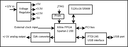
This is the block diagram for the hardware
The Schematic and Layout files are here. Note that there are some errors with the design and symbols that are described in the mistakes.txt file.
The tools I used don't have any of the error checking that most other tools have, but they're free and the boards produced are cheap. There are a couple of hitches: there is no way to split power planes, and the minimum outline radius is greater than the slot size of the PCI connector. I marked the slot positions with traces, and used a dremel cut-off wheel to cut the slots.
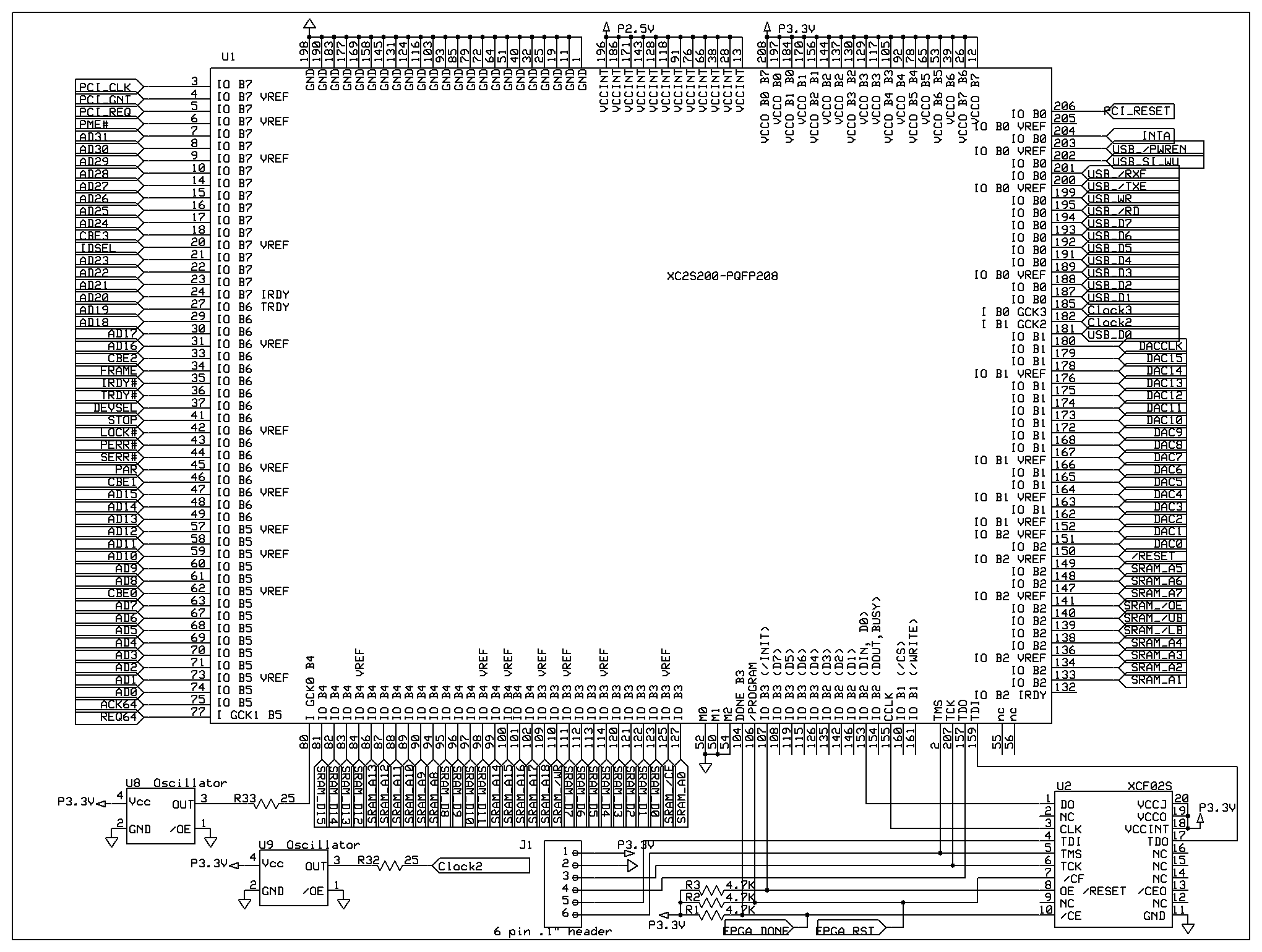
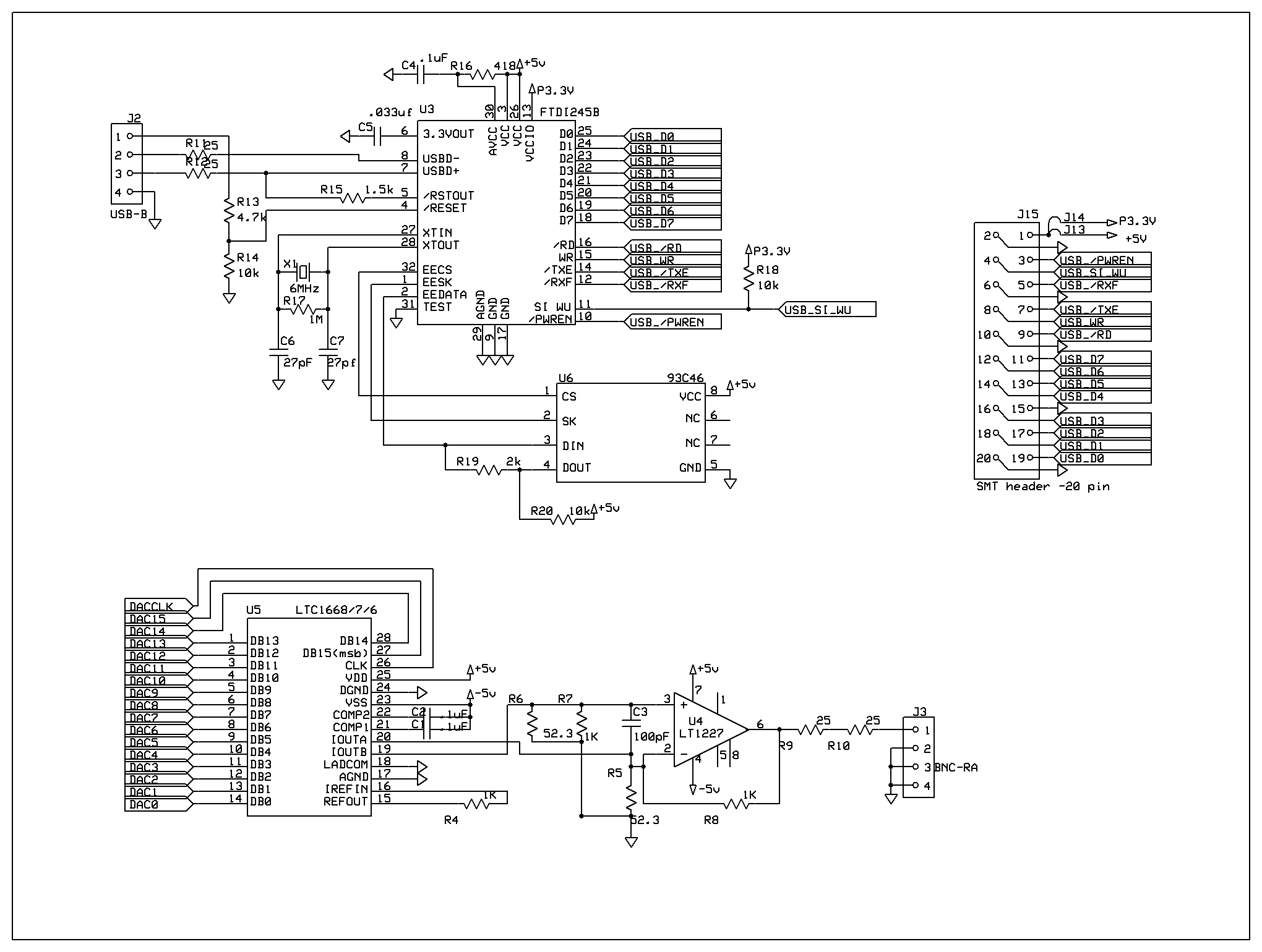
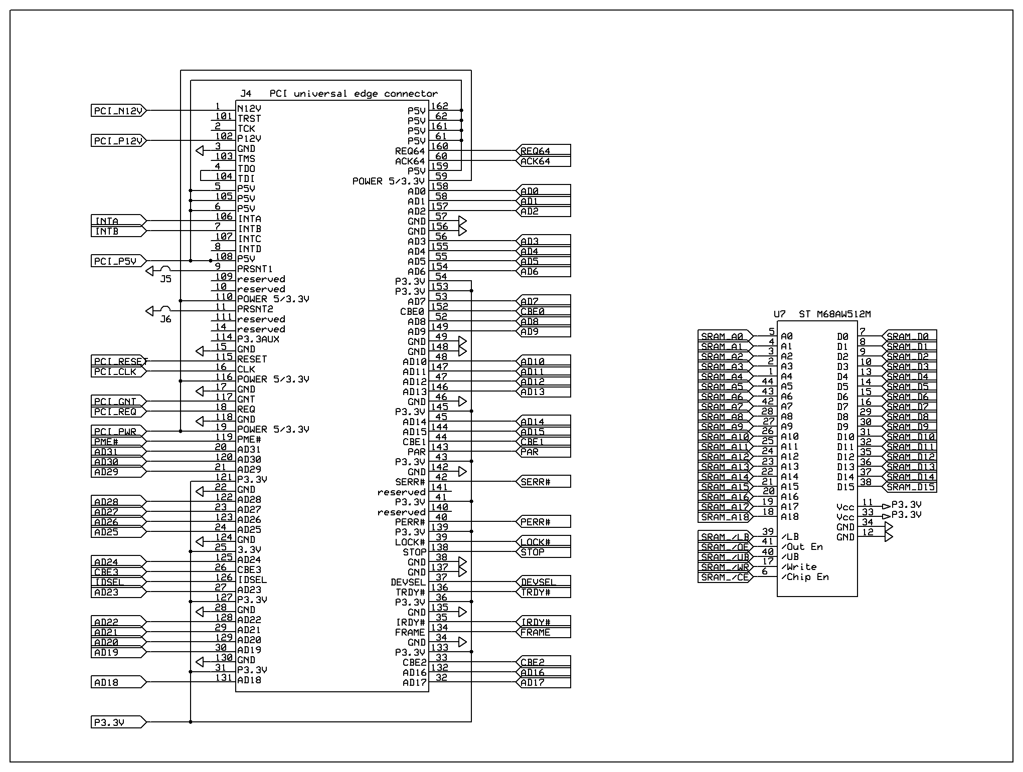
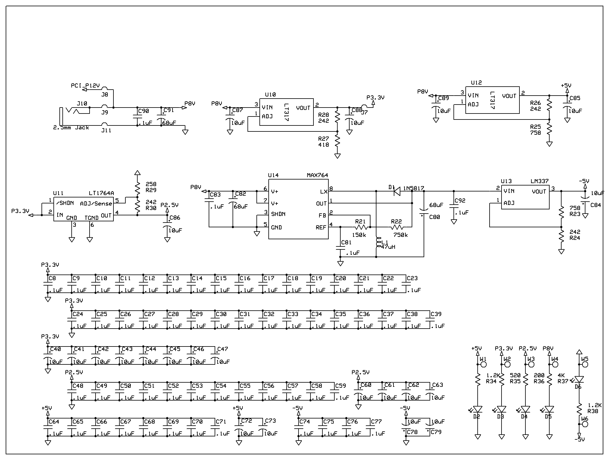
When I created the PCB, I wasn't sure which PCI signals were necessary, and I included too many. The DAC also uses too many lines. I designed the board with a 16-bit part in mind, but that was not available so I used the 12-bit version instead. With the noise from a common digital and analog ground plane, it is unlikely that the difference in resolution matters. The SRAM chip on one of my boards had bad address lines on data bits 5 and 6, so I swapped the lines with bits 0 and 1 in the .UCF pinout file. For real fun and games, replace the SRAM with DRAM.
Schematic pages:
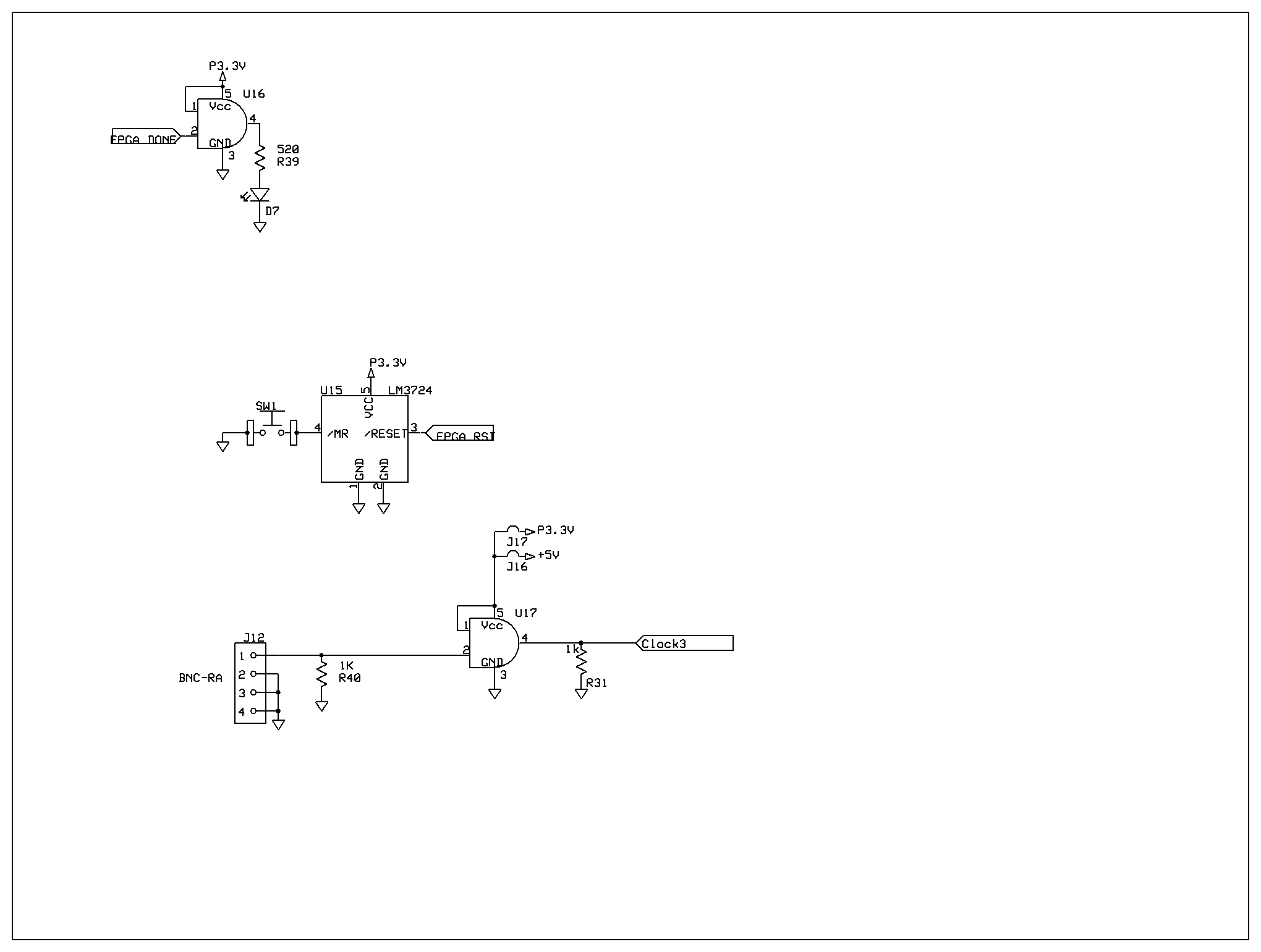
FPGA
FPGA support
DAC and USB
PCI and SRAM
Power
Here's the Finished board:
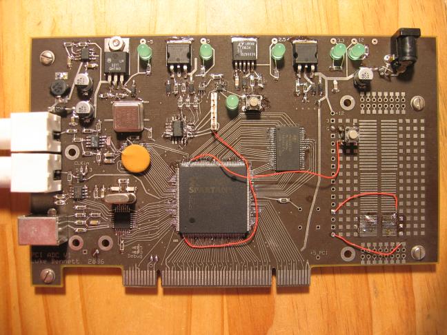
The output is one of the BNC connectors on the left side of the card, and the USB connector is below it. The card edge connector fits in a USB expansion connector as a 5/3.3V universal device. External power can be connected to the jack on the top right of the board.
The total cost was around $500 for two cards. The PCB cost $200 for a pair (minimum order) and the components around $300. It should be possible to reduce the cost by up to $100 with simple changes to component selection.