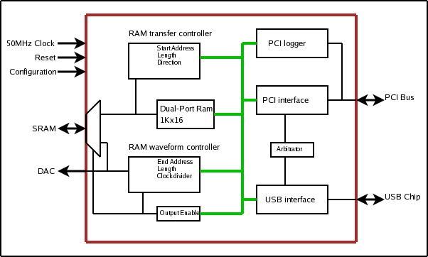
This is a block diagram of the internal structure of the FPGA. The green lines are the internal bus, whose signals start with "ib_"
Here are the FPGA source files:
simulation_level.v
	pci_emulator.v
	sram_emulator.v
	usb_emulator.v
	fpga_top_level.v
		fpga_top_level.ucf
		analyzer.v
		arbitrator.v
		dacdriver.v
		debouncer.v
		pci_interface.v
		usb_interface.v
All the code is written in Verilog. The module simulation_level is the top-level simulation module, and fpga_top_level is the module that should be synthesized to generate the FPGA configuration. The RAMB4_Sx_Sx_modified.v files are copied from the Xilinx package, but modified to not use the global reset line in the FPGA. The RAMB4 files must be included in the Modelsim project, but should not be included in the ISE synthesis project.
The FPGA design is centered around an internal buswith 16 data and 11 address lines. The bus is syncronous, with the clock line driven by the current master. The only non-obvious part of the bus operation is in a read operation: the peripherals respond to the address in the clock cycle before the read line is asserted. This is how the internal block ram operates, and the other registers emulate this behavior for consistency.
The dacdriver module does not allow direct access to the external SRAM, as it is far too slow for the PCI bus. Instead, data is written to a 1K word internal ram, and a state machine loads the data from the internal buffer to the external SRAM.
The USB interface is a state machine that listens for incoming characters on the USB port, then reads or writes data on the internal bus, and sends any read data back on the USB port. The packet format for the interface has a 20 bit address field, which is leftover from when it could directly access the external SRAM.